Cell-Based Design Flow
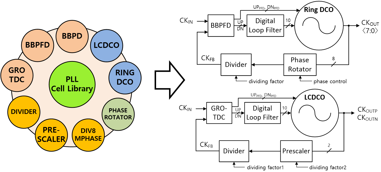
Cell-based design flow is a systematic design flow starting the design by verifying functionality of system model, and then turning it into circuits and layout. While traditional analog/mixed-signal circuit designers are suffering from high complexity of circuit system, this model-first design flow enables quick chip-level verification by XMODEL and automatic place-and-route (P&R) using IC Compiler and Custom Designer. With the aid of cell-based design flow, a person who may not aware of detail transistor-level circuit topologies can make PLLs without difficulty, only by model-level manipulation with provided analog cell library (ACL).
|
Tutorial Materials for Exercise
This material is an education-purpose package used in IDEC lecture on May 19-20th, 2016. This includes a digital phase-locked loop (PLL) example and ACL models to learn and exercise cell-based design flow for analog/mixed-signal IC. Also, it contains automated P&R scripts and libraries to experience IC Compiler/Custom Designer (ICCD) flow.
Please refer to the setup guide before you download the tutorial file package.
Setup guide: Easy_Setup_Guide.pdf
Tutorial file package: IDEC_CBDF.tar.gz
Lecture notes: lecture_notes.zip
(The setup guide and the lecture notes are appended to the tutorial file package: IDEC_CBDF/doc/)
|

